8+ Silicon Wafer Sds
Thickness 2 in. Sigma-Aldrich Canada Ltd 2149 Winston Park Drive OAKVILLE ON.
Download Block Gsi Helmholtzzentrum Fur Schwerionenforschung
ACCIDENTAL RELEASE MEASURES 61 Personal protection None.

. 14 rows Hyperpure silicon wafers are the basis for almost all semiconductor elements and consequently represent an essential basis for the worlds electronics industry. It provides information on proper handling storage and disposal of the chemical. An MSDS is a document that comes along with a hazardous chemical.
12 EN Revision Date. IDENTIFICATION OF THE PRODUCT AND OF THE COMPANY. 647101 Silicon wafer single side polished N-type contains no dopant diam.
Silicon wafers are Non-flammable. Silicon wafers are solid. Page 1 8 _____ Silicon Reference Standard Solution 1000ppm Certified.
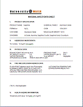
SI-E-02-WF SI-E-03-WF SI-E-04-WF SI-E-05-WF CAS. All applicable American Elements product codes eg. Product Wafer MSDS Rev 22 06012022 Page 1 of 4 Revision date 06012022 MATERIAL SAFETY DATA SHEET 10 IDENTIFICATION Product Name.
HANDLINGAND STORAGE 71 Handling. Product Name Silicon Reference Standard Solution 1000ppm Certified Cat No. Safety Data Sheet SiliconSilicon Dioxide Wafer ACS Material LLC Version.
Silicon element Linear Formula. Product Wafer MSDS Rev 30 06012022 Page 2 of 4 Revision date 06012022 MATERIAL SAFETY DATA SHEET 40 FIRST AID MEASURES Inhalation. 8 018µ Silicon Wafer.
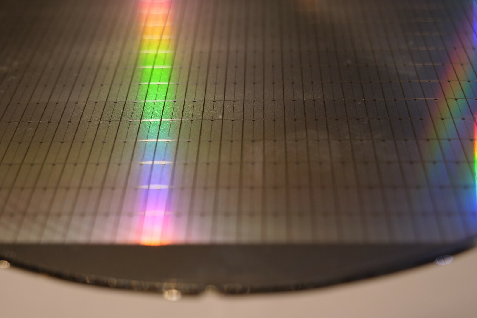
05 mm Synonym s. All Photos 1 R2R Monolayer small grain CVD graphene on silicon wafer. PRODUCT AND COMPANY IDENTIFICATION Product name.
Silicon Wafer Product Number. In soft lithography the fabrication of a mold often made in SU-8 is required for replicating PDMS microfluidic structures. For the fabrication of this SU-8 master a standard photolithography.
The SDS is standardized and requires.

Solvothermal Synthesis Of Zirconia Nanomaterials Latest Developments And Future Sciencedirect
Multilayer Assembly For Solar Energy Conversion Springerlink
Silicon Wafer 8 Inch Ebay

Conformational Change Initiates Dehydration In Fluconazole Monohydrate Crystal Growth Design
Magnetic Au Nanoparticles On Archaeal S Layer Ghosts As Templates Document Gale Academic Onefile
What Scientific Research Are Silicon Wafers Used For
For Si Wafer Msds Please Click Here

200mm Silicon Wafer 8 Inch Waferpro

Pdf On The Anomalous Peak In The Forward Bias Capacitance And Conduction Mechanism In The Au N 4h Sic Ms Schottky Diodes Sds In The Temperature Range Of 140 400 K Ahmet Kaya
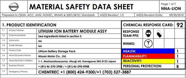
Material Safety Data Sheet Msds Defined

Silicon Wafer American Elements

Tailoring Porous Silicon For Biomedical Applications From Drug Delivery To Cancer Immunotherapy Li 2018 Advanced Materials Wiley Online Library

Genesis And Tuning Of Ferromagnetism In Sno2 Semiconductor Nanostructures Comprehensive Review On Size Morphology Magnetic Properties And Dft Investigations Sciencedirect

Solvothermal Synthesis Of Zirconia Nanomaterials Latest Developments And Future Sciencedirect

8 Inch Test Grade Silicon Wafer China Silicon Wafer And Test Garde Wafer

Silicon Wafers Preparation And Properties Sciencedirect

Genesis And Tuning Of Ferromagnetism In Sno2 Semiconductor Nanostructures Comprehensive Review On Size Morphology Magnetic Properties And Dft Investigations Sciencedirect